Spatial Atomic Layer Deposition
To battle climate change, we need to rapidly transition to a sustainable way of generating, storing, and converting energy. High-performance electrolysers for green hydrogen and fuel cells, batteries, and solar cells are part of the solution. However, these technologies still face major challenges in performance, lifetime, circularity, and use of scarce and critical materials.
Revolutionary new technology is required to tackle these challenges and ensure a sustainable energy future. One of these new technologies is spatial Atomic Layer Deposition (spatial ALD).
Spatial ALD offers the ability to deposit ultra-thin layers at higher deposition rates, while highly reducing the use of scarce materials, and maintaining excellent performance.

How does spatial ALD technology work?
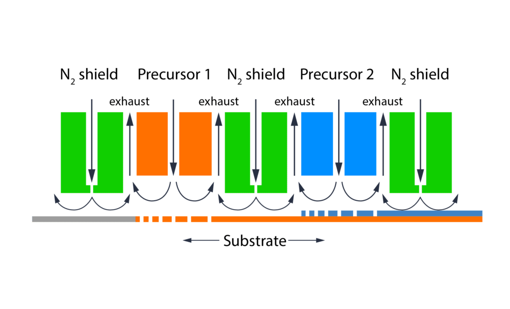
Spatial Atomic Layer Deposition is a variation of the traditional Atomic Layer Deposition (ALD) technique. While conventional ALD is a time-sequential, cycle-based process that involves the repeated exposure of a substrate to different precursor gases in a controlled sequence, spatial ALD uses a spatial separation of these precursor exposures. In spatial ALD, the precursors are physically separated in space rather than being introduced sequentially. In SparkNano’s proprietary design, the spatial ALD tools can be seen as a “printer” where instead of ink, the precursor gases are locally dosed, printing ALD films.
To the right, a schematic drawing of spatial ALD reactor concept: where the precursor and the plasma (co-reactant) zones are spatially separated by inert gas shields. The two half-reactions will take place subsequently to form an ALD monolayer, by moving the substrate underneath the reactor. Thicker layers are obtained by repeating the movement.
What is Traditional ALD?
Before going into spatial ALD, we’d like to take a look at the traditional way of Atomic Layer Deposition. We will discuss the methods used, the presented challenges and how spatial ALD presents the solution.
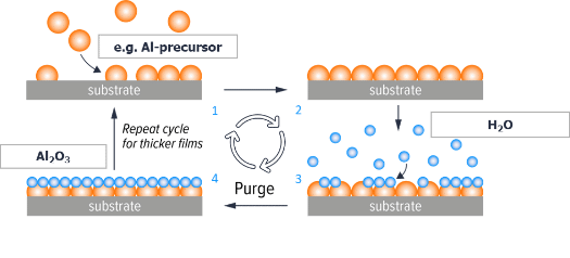
Traditional Atomic Layer Deposition (ALD) is a thin-film deposition technique used in the manufacturing of semiconductors, integrated circuits, and various other types of electronic devices. It is a process that allows for precise control over the thickness and composition of thin films at the atomic level. The key characteristic of ALD is its layer-by-layer deposition method, which involves the sequential exposure of a substrate to reactive gases called precursors, in a cyclic fashion. The precursors react with the substrate surface where one atomic layer of material is deposited per cycle. The process is typically carried out in a vacuum environment.
Atomic Layer Deposition is widely used to make cutting-edge computer chips, because of the unique way it deposits complex materials, with atomic-scale control of the material composition, uniformity, and quality even inside highly complex 3D structures. For the same reasons, Atomic Layer Deposition can be used for industrial-scale manufacturing of the next generations of sustainable energy devices.
How does Traditional ALD work?
The ALD cycle consists of the following steps:
Substrate Preparation
The coated substrate is loaded into the deposition chamber and typically heated to a specific temperature. The temperature is crucial as it influences the kinetic reactions and the quality of film growth.
Precursor 1 Exposure
The first precursor gas is introduced, and it reacts with the substrate surface, forming a monolayer. Precursors are dosed continuously, at the same time, but in different zones.
Purge
Excess precursor and by-products are purged from the chamber.
Precursor 2 Exposure (plasma/co-reactant)
The second precursor gas is introduced, reacting with the newly formed monolayer. Precursors are dosed continuously, at the same time, but in different zones.
Purge
The chamber is purged again, completing one cycle.
The advantages and challenges of Traditional ALD
Traditional ALD offers several advantages, including excellent conformality, precise control over film composition, thickness, uniformity, and the ability to deposit high-quality thin films on a variety of substrates. These qualities make ALD particularly suitable for applications requiring precise control of film properties, such as in the semiconductor industry, but also for next-generation electrolysers, fuel cells, batteries, and solar cells.
However, the challenges of conventional ALD for these applications are:
- It requires a vacuum, which makes ALD on large and flexible substrates complex and expensive
- It is difficult to scale up to large-sized substrates and roll-to-roll
- ALD makes inefficient use of costly precursors
- ALD is slow; it can take hours to deposit
By using spatial ALD these challenges can be tackled.
Would you like to know more about spatial ALD? Feel free to contact us.
The advantages of spatial ALD
Upon the advantages that Traditional ALD offers, SparkNano’s spatial ALD approach offers many additional advantages:
Atmospheric pressure
No vacuum is required; it works at atmospheric pressure but in inert environments. This means no vacuum pumps and no load locks.
Scalability
It can be scaled up to very large substrate sizes and even continuous roll-to-roll processing on flexible foils.
Efficiency and reduced waste
As spatial ALD is used as a printer, films are only deposited where they need to be. No deposition on reactor walls or unwanted surfaces. This means less precursor wastage and less downtime. We can do direct patterned deposition; no masks, no pre- or post-treatment, and less precursor wastage.
We can reclaim unreacted precursor for recycling; this further maximizes precursor utilization to >95%.
Increased throughput and reduced cycle time
It is done fast: deposition rates are 100x faster than for conventional ALD, which means that hours become minutes.
Applications of spatial ALD
Hydrogen
Spatial ALD can be used to coat electrodes, porous transport layers (PTL), gas diffusion layers (GDL) and membranes for electrolysers and fuel cells. Examples include thin catalyst layers (e.g. iridium oxide and platinum) on high surface area supports to reduce the precious metal loading 10-50x times while maximizing the electrochemical performance and stability. Other uses include coating anti-corrosion layers on electrodes to increase stability and lifetime.
Deposition possibilities available are e.g. Ir / IrO / Pt
Batteries
Spatial ALD can be applied to coat battery electrodes with an ultrathin and uniform layer of materials, enabling improved energy density, charge time, safety, and lifespan of rechargeable batteries. These coatings can have a thickness from a few atoms to several nanometers. Also, new battery concepts like solid-state and 3D batteries will benefit from ALD coatings.
Deposition possibilities available are e.g. AlOx / Nboxide / LIF
Solar cells
Spatial ALD can be used for depositing passivation layers in c-Si solar cells, encapsulation layers in various thin-film solar cells, and interface layers in perovskite-based tandem cells, all meant to either increase efficiency or improve the lifetime of the solar cells.
Deposition possibilities available are e.g. AlOx / SnO2 / ZnO
SparkNano’s spatial ALD Tools
SparkNano’s product range includes versatile and flexible R&D tools for process development and pilot production (LabLine™) series and tools for mass production on planar, porous, and flexible substrates, either via sheet-to-sheet (Vellum™) or roll-to-roll (Omega™) series, respectively.