Spatial ALD: a thin film deposition method
Thin layer deposition, also known as thin film deposition, refers to the process of depositing a very thin layer of material onto a substrate or surface. These deposited films can be just a few atoms or molecules thick. The goal of thin layer deposition is to modify the substrate’s (sample) surface properties or create functional coatings with specific characteristics. This process is used in various industries.
Thin layer deposition is essential for the manufacturing of devices such as integrated circuits, fuel cells, solar cells, optical coatings, and more.
Thin film deposition methods
Thin layer deposition methods include techniques such as Spatial Atomic Layer deposition (ALD). Spatial ALD is an advanced variation of the traditional ALD technique. In conventional ALD, thin films are deposited by sequentially exposing a substrate (planar, porous, or flexible) to two or more gaseous precursors (substances).
Thin layer deposition method: Spatial ALD
Instead of using sequential exposures, spatial ALD offers several advantages over traditional ALD methods for thin film deposition. By using separated precursor sources for each chemical reaction and introducing the precursors simultaneously but in separate spatial regions on the substrate (sample), spatial ALD allows for more uniform coatings. This uniformity is essential, especially in applications requiring precise and consistent thin films.
The evenness of the deposited layers not only enhances the material’s functional properties but also contributes to the overall performance and reliability of the devices or systems in which these materials are used.
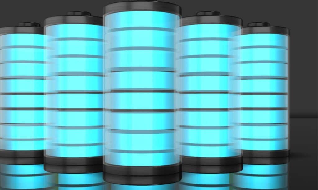
Uniform coatings are essential for ensuring consistent electrical, optical, or mechanical properties, which are critical for the functionality and longevity of electronic components and devices, such as hydrogen, batteries, and solar cells.
Applications in thin film deposition

Hydrogen electrolysis and Fuel cells
Thin film deposition has various applications, including hydrogen electrolysis and fuel cells. By reducing the amount of iridium and platinum on the Porous Transport Layer (PTL) of a Membrane Electrode Assembly (MEA), costs for water-based hydrogen electrolysis and fuel cells can be significantly decreased. This breakthrough is achieved by minimizing the use of these precious and expensive metals, up to 40 times less than before.
Passivation layer for Cathodes for batteries
For batteries, a thin layer serves as a passivation layer for cathodes (an object that electricity moves through). A passivation layer is a metal finishing process which protects the cathode against corrosion. This is crucial for improving the durability and longevity of batteries, making them more reliable and cost-effective in the long run.
Making thin film deposition possible
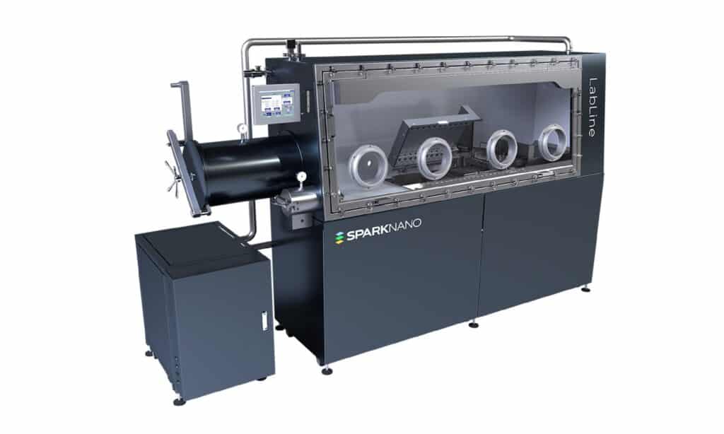
Tools from lab to fab
SparkNano’s product range includes versatile and flexible R & D tools for process development and pilot production (Labline series) and fab tools for mass production on porous and/or flexible substrates, either via sheet-to-sheet or roll-to-roll (Vellum & Omega series respectively).
Each product is based on atmospheric pressure spatial ALD, either thermal- or plasma-enhanced.