
Spatial ALD: Mask-less patterning & High deposition rate
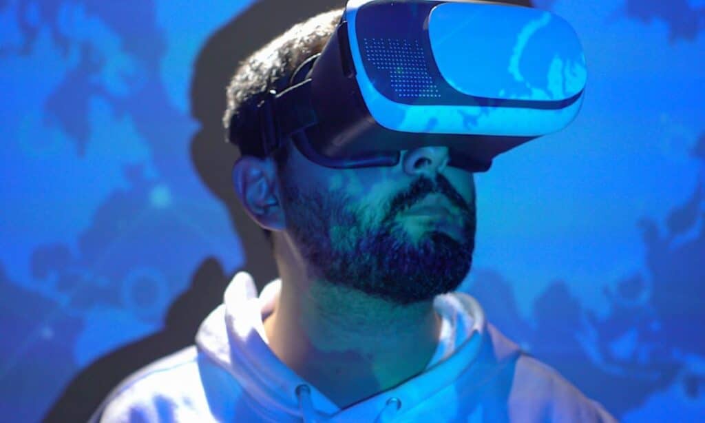
Spatial ALD is famous for the dense, conformal and pinhole-free films that can be deposited using this technology. This is why Spatial ALD is used in various opto-electronics applications, such as encapsulation layers in OLED devices, sidewall passivation for MicroLED devices, high mobility oxide semiconductors for thin-film transistors and optical layers in waveguides for AR/VR devices.
SparkNano offers the best R&D and mass production solutions for these applications through the high deposition rate and excellent conformality realized by Spatial ALD in combination with SparkNano’s mask-less patterning technology.
Layer deposition on 3D structures
Current technology not able to deposit encapsulation layers on complex 3D structures
Plasma enhanced Spatial ALD can deposit uniform layers on 3D structures at low temperature

High refractive layers
Current challenge is Light coupling without losses in AR/VR glasses and waveguides
Spatial ALD offers high refractive layers with excellent 3D conformal deposition with patterning